Case-Study Case-Study, RF, DSP, Signal Processing
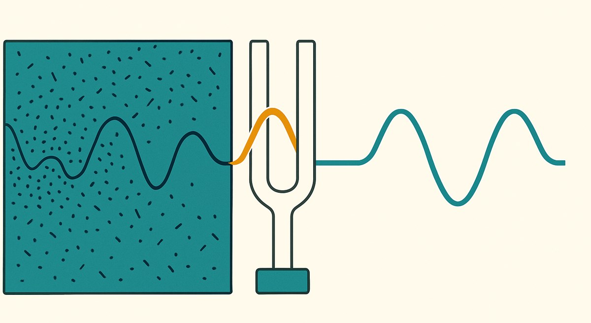
A large family of measurements does not deliver its information at DC. It arrives riding on a carrier: the free induction decay of an NMR or EPR experiment, the response of a resonant sensor driven at its resonance, the return of a swept optical or acoustic interrogator, the output of an RF front end. The quantity you actually want, the slowly varying amplitude and phase of that carrier, occupies a few kilohertz. The carrier sits at several megahertz.
The traditional answer is an analog quadrature demodulator: two mixers, a local oscillator, two low-pass filters and two ADCs. It works, and it brings with it everything analog hardware brings, namely gain and phase imbalance between the I and Q paths, DC offsets that drift with temperature, and a set of components that has to be re-tuned whenever the carrier frequency changes.
The alternative is to digitise the carrier directly and do the whole conversion in the FPGA. That is what the RF plugin is for.

The chain
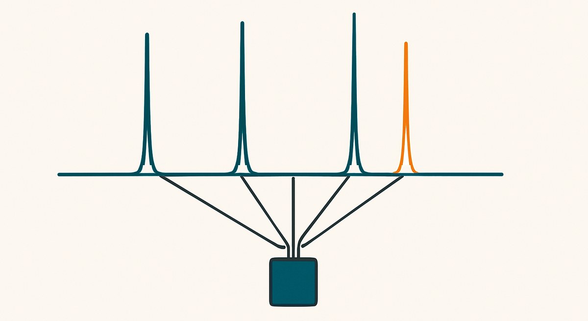
NCO. A numerically controlled oscillator emits a complex I/Q sinusoid at the local-oscillator frequency. Because it is generated arithmetically, the I and Q components are exactly 90 degrees apart, by construction, forever. There is no quadrature error to trim and no drift to track. Two variants exist: a fixed-frequency NCO, where the frequency is baked into the netlist at synthesis, and a programmable one that takes a tuning word at runtime, which is what you want if the carrier can move or if you need to sweep.
Mixer. A sample-by-sample complex multiplier. Each of its two inputs can independently be real or complex, and so can its output, which matters here because the ADC delivers a real stream and the NCO a complex one. The product contains the wanted signal translated down to near zero frequency and an unwanted image at twice the carrier. The image is the reason the next stage exists.
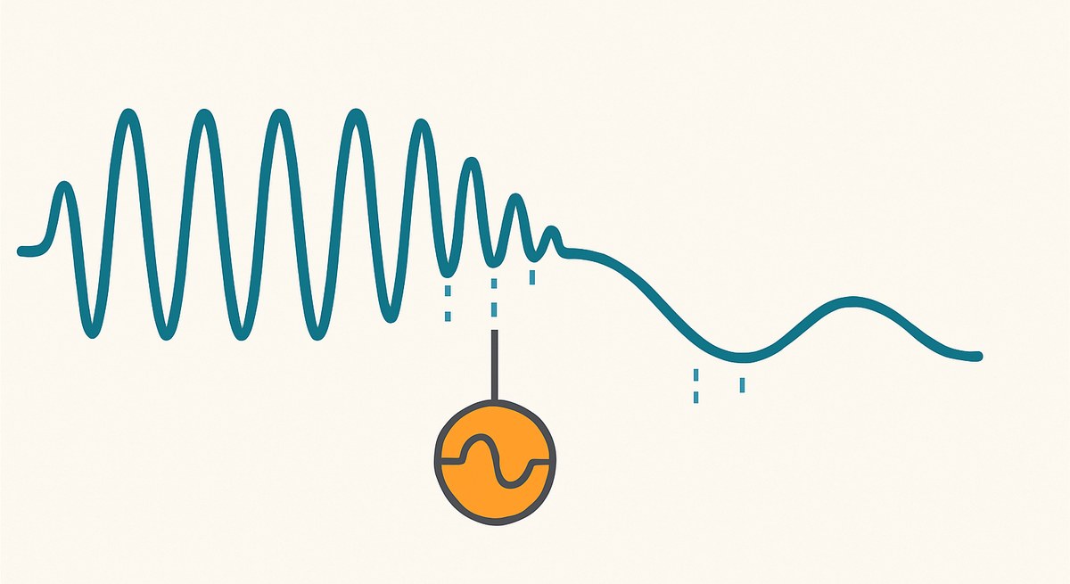
CIC Decimator. A cascaded-integrator-comb decimator is the cheapest anti-alias filter that exists in an FPGA: integrators and combs, no multipliers at all. It removes the image and drops the sample rate by a large factor in one step. Doing this early is the whole economic argument of the chain, because every stage downstream now runs at a fraction of the ADC rate and therefore costs a fraction of the hardware.
CIC + Compensator. The CIC is cheap because its response is a cascade of sincs, and a cascade of sincs is not flat. It droops across the passband, and the droop gets worse the more stages you use to buy stopband attenuation.
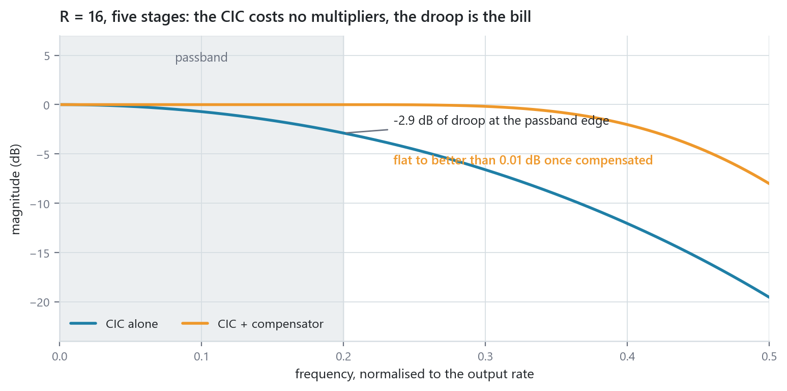
At a decimation of 16 with five stages, the response is already almost 3 dB down at the edge of a passband taken as 40 % of the output Nyquist. Three decibels is a factor of two in power, silently applied to your measurement as a function of where in the band it happens to sit.
The compensator is a short FIR that runs at the low output rate and whose response is the inverse of the droop over the passband. Because it runs after the decimation, it costs a handful of multipliers instead of a bank of them. In the block this is not something you assemble yourself: the CIC + Compensator Decimator is a single block that contains the CIC, the compensating FIR and the DC gain normalisation, and what comes out the far side has a flat passband and unity gain.
CORDIC. The last step turns the complex baseband sample into the two numbers the experiment is actually about: magnitude and phase. The CORDIC does it with shifts and adds, no multipliers and no arctangent table.
Why the two-stage decimation
It is tempting to do the rate reduction in one FIR. The reason nobody does is arithmetic. A FIR sharp enough to protect a narrow band after a decimation of, say, 256 needs a tap count in the hundreds, and at the full ADC rate every one of those taps is a physical multiplier running at 125 MHz.
Splitting the job changes the bill completely. The CIC removes the bulk of the band at zero multiplier cost. The compensator, and any further sharpening, runs after the rate has already dropped, where one physical multiplier can be time-shared across many taps. The Multi-stage FIR Decimator takes this idea to its conclusion: you give it input and output sample rates, a passband edge and a stopband attenuation in engineering units, and it factorises the ratio into up to four stages, designs a Kaiser-window filter for each, and shows you the resource estimate in its designer before you commit.
What the designers do
Three of these blocks open a graphical designer on double-click: the FIR Designer, which is a Matlab-like filter toolbox with the response plotted live; the CIC Decimator Designer, which shows the cascade response and the droop you are about to accept; and the Multi-stage FIR Decimator Designer, where the per-stage decimation factors and transition bands are editable and the resource estimate updates as you move them.
This matters more than it sounds. The hard part of a DDC is not the arithmetic, it is choosing the decimation split and the transition bands so that the thing both meets the specification and fits in the device. Doing that with the response and the resource count in front of you is a different activity from doing it on paper.
What you get
The output is a complex baseband stream at a rate matched to the bandwidth you actually care about, with the amplitude and phase already extracted, in a chain with no analog quadrature error, no DC offset drift, and a local oscillator frequency that is a register write rather than a component change.
This is a reference design. The chain and the block behaviour are as documented; the figures are computed from the models described, not measured on an instrument.